 Features of QR400K
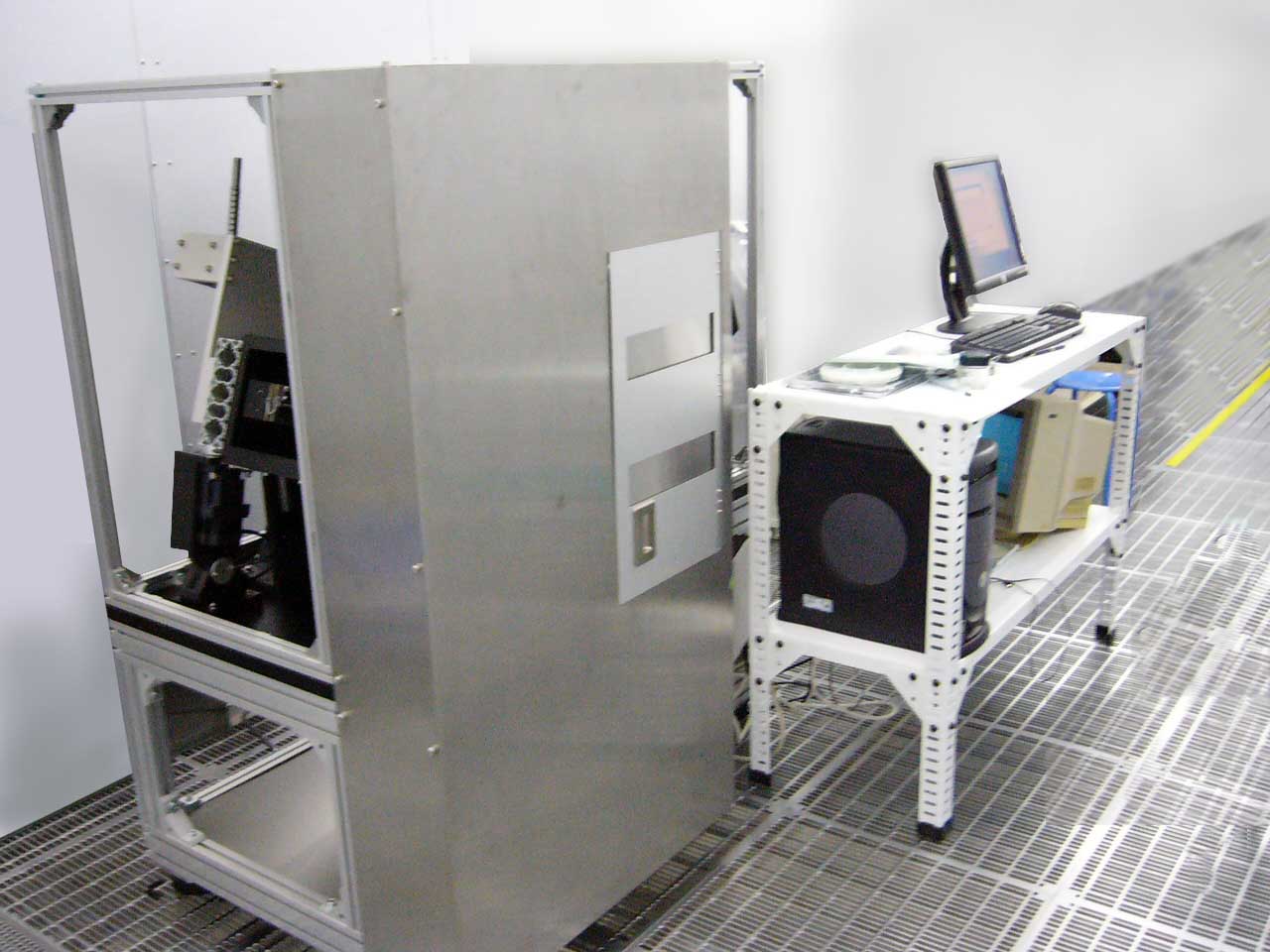
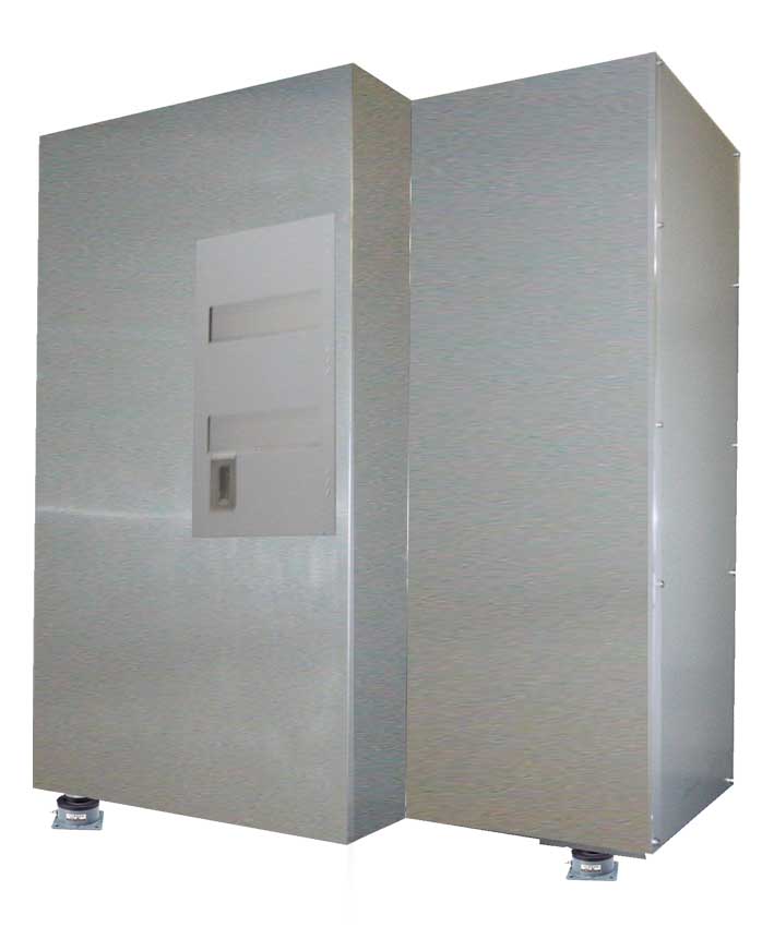
Heureka Co., Ltd. has developed surface analysis device QR400K that has the functions of the film thickness inspection, the film quality inspection, and the macro inspection in the semiconductor inspection field, and now starts to offer the device.
QR400K is the surface analysis device for 200mm wafer with the functions of two dimensional ellipsometer and the macro defect inspection, which can collectively measure all aspects of the wafer. Under the united inspecting standard, QR400k enables to track and manage the characteristic of the film by high accuracy in all stages of the semiconductor process.
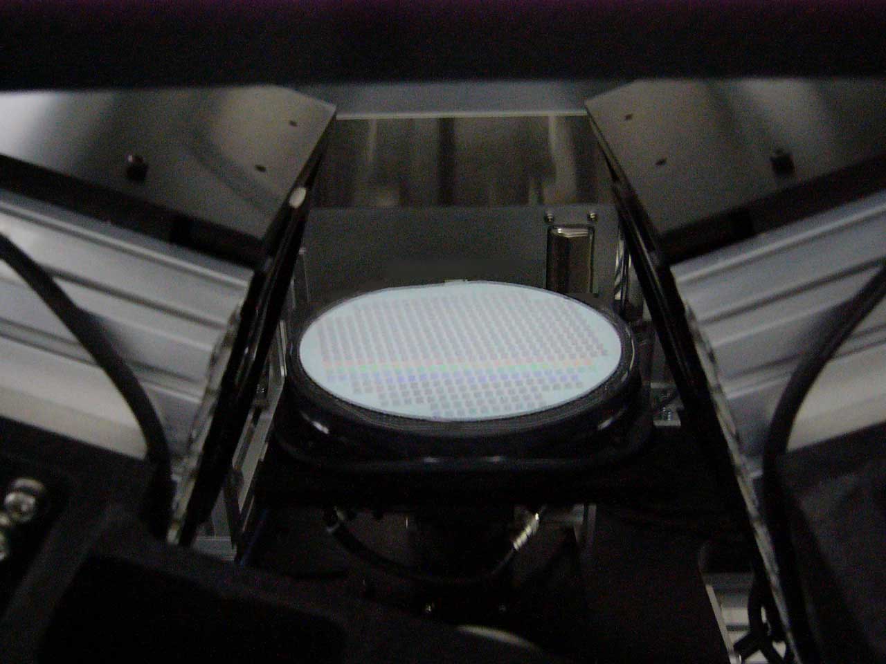
QR400K has achieved the performance of the highest degree as an ellipsometer. It measures the refractive index and the thickness of the thin film in two dimensions and displays the result as an image. To improve the measurement accuracy and shorten the calculation time of the multilayer film, it measures by two wave length (650nm and 785nm). The angle of incidence that enables the best accuracy will automatically be set by the resolution of 1/100000. Moreover, it has the function of the self adjustment of the measurement standard coordinates. The all aspects of 400,000 points on the 200mm wafer can be measured by surface resolution of 100μm in 30 seconds. (It can go up to surface resolution of 10μm according to the zoom mechanism of the option. )
The funcions of learning and the image data processing developed through the measurement of the quality items enable this device to detect geometrical features of the sample by high throughput. In addition, this device can detect the defect of 20オm or more (standard) by measuring the diffraction light caused by a warp, an irregular film, and garbage, etc.
By applying two techniques of the ellipsometry and the defect detection to one sample at the same time, the measurement factors that could not be separated up to now can be clarified. Thus, the device can separately detect the geometrical features such as dust, damages, or warps and the physical features such as thickness or quality alteration of a film.
The main specifications
| Size of wafer |
200mm
|
| Throughputs |
120 pieces/hour (ellipsometry) 100 pieces/hour (defect inspection)
|
| Major target of inspection |
thickness and quality of transparent film, geometrical shape of sample pattern
|
| Size (WラDラH) |
1340×860×1570 mm
|
| Weight |
300kg
|