2-dimension ellipsometer BEPE and MFE algorithm can measure multi-layer film with huge amount of data. BEPE is not only doing measurement of the refractive index and film thickness based on given model of the sample as conventional ellipsometer do, but also be a tool for searching the structure of samples. The true nature of inside structure , which we were naming obscure word 'VOID’, is revealed ,too.
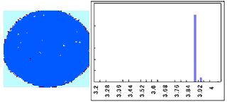
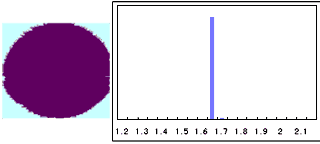
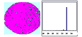
The following is a report on optical character of Polysilicon film used for PBS, measured by the machine BEPE QR120K.. Polysilicon film on the thick oxide layer can be measured easily.(Figure 1) However, the optical character of Polysilicon film on Silicon substrate have not been measured definitely, because the refractive index of Polysilicon and that of Silicon is almost the same.
BEPE can measure optical character of Polysilicon on Silicon, for it can measure refractive indexes of samples with high accuracy.
We measured Silicon wafers of 150mm diameter. Front surface is mirror polished, and back side is etched surface. For the experiment, Polysilicon films are deposited on the both side of Silicon wafer. At this time ,the native oxide on Silicon substrate was not removed. We measured 3 types of samples ,each includes 6 wafers whose thickness is different. We will report about the sample of 1.2μm thickness, for they have essentially the same nature despite their different thickness.
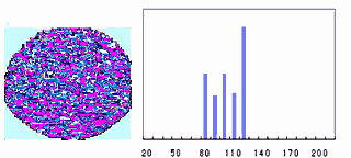
Fig.1 Polysilicon film on the thick oxide layer
(Polysilicon 1.2μm/SiO2 0.3μm/Si) |
|
|
|
Treating polysilicon as monolayer film, we can not get any solution by ellipsometric calculation. Next by treating as 2-layer film, we can get acceptable results about film thickness and refractive index as a whole but the refractive index of the nearest layer to the substrate point out strange outcome.
In Ellipsometry it is also important information that the solution can not be gained. It suggests that actual sample has more complicated structure than we have ever thought.
Refractive index relate to dielectric constant and density of substance. Therefore we can estimate the structural changes or compositional ones of film with the direction of thickness by looking over the distribution of refractive index.
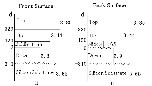
Finally we treat the polysilicon as fourfold layer - by the surface, Top,Up,Middle,Down/Substrate and tried analyzing.
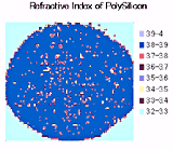
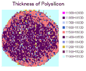
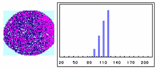
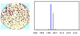
Fig.2 Structure of Polysilicon on Mirror Polished Silicon Substrate
| Refractive Index | Thickness |
|---|---|
 |  |
| Top Layer | |
 |  |
| Up Layer | |
 |  |
| Middle Layer | |
 |  |
| Down Layer |
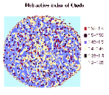
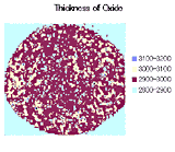
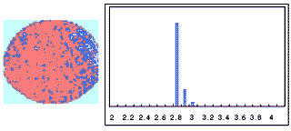
Fig.3 Structure of Polysilicon on Etched Silicon Substrate
| Refractive Index | Thickness |
|---|---|
 |  |
| Top Layer | |
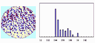 |  |
| Up Layer | |
 |  |
| Middle Layer | |
 |  |
| Down Layer |
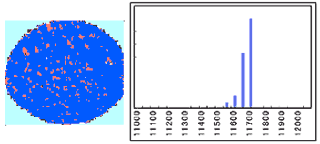
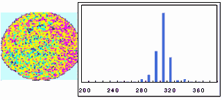
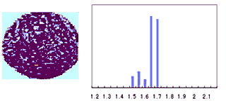
Now we are interested in the phase relation between the thickness of Middle Layer and Down Layer. Here we call the composed layer with Middle Layer and Down Layer as Inter facial Layer. Fig.4 shows the distribution of the thickness of Interfacial Layer.
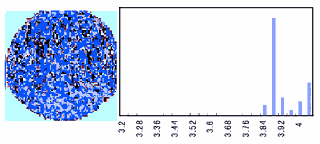
The distribution of thickness of Interfacial Layer deposited on back surface is considerably broader than that on front surface. The variance of thickness of Interfacial Layer may be explained by flatness or low-frequency components of micro roughness of Silicon surface. This results can be read as following. Among the Interfacial Layer, Down Layer close to substrate is still affected by roughness of the substrate and coming to the Middle Layer the surface become almost flat.
Through this analysis, we can find out how is the structure of interfacial layer between Polysilicon and Silicon affected by the roughness of silicon substrate surface. The roughness of the surface of Silicon substrate is appeared as the variance of the thickness of Interfacial Layer at this stage of analysis.
Fig.4 Thickness of Interfacial Layer
| Front Surface | Back Surface |
|---|---|
 |
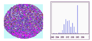 |
Fig.5 Analyzed model of Polysilicon film
Thus the reality of the sample is gradually made clear.
We can set the structure like Fig.5 as the sample model.
What causes these optical phenomena?
Are Grain sizes changing belong to thickness?
How relates to process parameters?
How is Gettering effect to the character of device?
Making use of BEPE series and MFE algorithm presented by HEUREKA, we can find the new subjects to investigate.